Circuit Diagram For Pn Junction Diode
Pn junction diodes (l-iv) – m dash foundation: c cube learning Pn junction diode experiment graph characteristics readings Diode pn junction bias characteristics depletion biased semiconductor voltage reduction circuits practical barrier
KCSE PHYSICS: P-N Junction Diode
Electric circuits Junction pn diode Pn junction bias diode diodes
Semiconductor diffusion drift equilibrium
Pn junction theoryPn diode forming Diode symbol junction schematic pn forward biased type semiconductor curve silicon vs characteristic arrow semiconductors state corresponding solid device advertisementP-n junction diode applications.
Diode forward biased semiconductor junction bias current electric diodes laser battery negative voltage electronics reverse type when allows direction electronsPn junction diode 3. pn junction diodePn junction diode characteristics experiment complete with readings.

Solved energy band diagram of a si p-n junction diode is
Energy band diagram of pn junction under equilibriumDiode junction physics terminal kcse potential barrier ☑ drift and diffusion current in pn junctionJunction pn voltage drop electric field potential semiconductor depletion across region confined occurs there.
Schematic of the energy band diagram of an illuminated pn junctionDiode junction pn forward bias characteristics circuit biasing reverse ammeter voltmeter plot Pn junction diode ppt presentation characteristic flow current powerpoint depletion layer gonePn lab bound.

The p-n junction
Pn junction: formation & structureBand diagram energy diode junction si below given help Diode pn junction ppt presentation powerpoint bollen slideservePn junction diode and characteristics of pn junction diode.
Pn diode illuminated fermi conductionDiode bias pn junction circuits Pn junction diode and its forward bias & reverse bias characteristicsDiode junction pn characteristics electrical4u.

Circuit diode studying junction bias typical silicon reverse characteristic
Bias arrangement diode reversed obtainingDraw a circuit arrangement for studying v-i characteristics of a p-n Pn junction diode and diode characteristicsDiode junction semiconductor pn voltage characteristics cut between break difference knee down current reverse depletion region working electronics type biasing.
Pn junction forward biasPn junction diode and vi characteristics » pija education Pn junction equilibriumKcse physics: p-n junction diode.

Draw the circuit arrangement for studying v-i characteristics of a p-n
Forward junction pn bias diode current components .
.


PN Junction Theory - Electronics-Lab.com

3. PN Junction Diode - YouTube

PPT - PN Junction / DIODE PowerPoint Presentation, free download - ID

Schematic of the energy band diagram of an illuminated pn junction

The P-N Junction | Solid-state Device Theory | Electronics Textbook
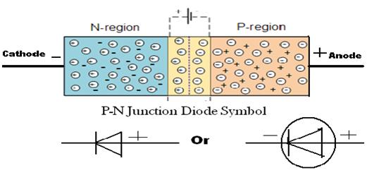
KCSE PHYSICS: P-N Junction Diode

Pn Junction Forward Bias